Effects of Trace Metals (Impurities) in Chemicals Used in Semiconductor Manufacture and Their Analysis
The original article by Yukihisa Kawada of the FUJIFILM Corporation, appeared in an e-newsletter of FUJIFILM Wako Pure Chemical Corporation and was translated by the company.
Ultra-high-purification technology required
In recent years, the manufacturing process for semiconductors has become increasingly complex in order to meet the technical requirements for smaller size and higher performance. In this situation, quality problems have been increasing, making it difficult to raise the yield rise and maintain the same level of stable production as previously.
The greatest difficulty resides in the detection of defects that can influence the yield and the identification of the substances responsible for the defects. Since the manufacture of semiconductors involves the use of many pieces of equipment and chemicals that are related to each other in complex ways, defects and their causes cannot be detected or identified without the cooperation of manufacturers. Therefore, to reduce the risk of causing defects, all items involved in the manufacture of semiconductors, from chemicals to equipment and its parts, are subject to strict quality control throughout the entire supply chain.
Regarding the products used in FUJIFILM Corporation' electronic materials (EM) business, increasing demands for "ultra-high-quality=ultra-high-purity" chemical solutions necessitate technical development in the area of chemical purification. However, evaluation technology (quality assessment) for the ultra-high level of purity aimed at is yet to be established, posing a problem for the entire semiconductor industry.
The International Roadmap for Devices and Systems (IRDS) was formulated to replace the International Technology Roadmap for Semiconductors (ITRS), which had served as a technical development guide in the semiconductor industry for an extended period. The IRDS specifies the detection and classification of multiple critical defects and S/N ratios in yield improvements as short-term key issues that need to be addressed no later than 2023.
One reason for the difficulty in detecting and classifying defects is that the sizes of defects to be controlled are getting smaller and smaller due to the trend towards semiconductor miniaturization. The latest 2018 version of the roadmap was published in July 2019, stating that the size of electrically active microparticles (mainly metal) on wafers that will be required in 2020 is 3.5 nm, a level which makes detection difficult using commercially available equipment only; just the inspection method itself poses a technical problem.
Effects of trace metals (impurities) and their analysis
To ensure ultra-high quality, it is necessary to control trace metals. Trace metals remaining in the chemical solution are potential sources of abnormalities in the electrical properties and processed shape. Therefore, strict process control is required to eliminate as many trace metals as possible. If any metal impurities remaining in chemical solutions used in the photolithography process, e.g., resists, thinners, developing solutions, rinsing solutions, as well as lower-layer materials, appear in or on the pattern, processing abnormalities can occur in the subsequent etching process. We have developed our own inspection method to prevent our liquid chemical products from causing quality problems in customer processes.
However, any evaluation to detect critical defects on the wafer, such as processing abnormalities (Fig. 1), requires many special devices and process materials.
Accordingly, the most common method for measuring trace metals used by chemical suppliers is to test chemical solutions using inductively coupled plasma mass spectrometry (ICP-MS). This technique has the highest sensitivity for general measurements, enabling us to achieve impurity control at the single-digit ppt level. However, when controlling trace metal concentrations in the chemical solutions, it is necessary to find out how the yield or critical defects on the wafer are correlated.
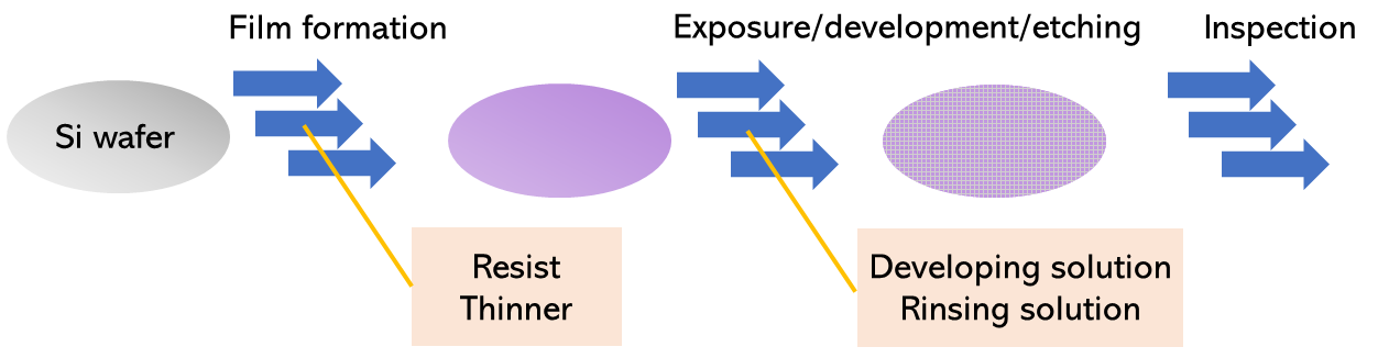
Fig. 1 Defect inspection sequence
Past and present trends in quality control
Priority products in our EM business include argon fluoride (ArF) immersion resists. A lithography process with an ArF immersion resist came into commercial use in 2007 using 45-nm nodes. However, quality control at that time required only single-digit ppb levels for trace metals.
In general, manufacturing equipment, facilities, and operations requiring human workers are potential sources of contamination and metal elements that need to be controlled include Al, Ca, Cr, Cu, Fe, K, Mg, Mn, Na, Ni, and Zn. Some semiconductors or chemical solutions have more than 20 elements that need to be controlled.
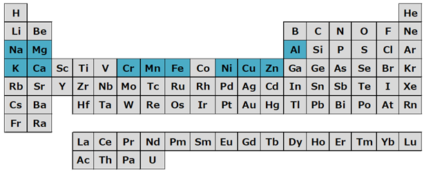
Fig. 2 Commonly controlled metal elements
However, because the development of 22-nm nodes led to increased miniaturization, making the process more complex and requiring more new chemicals, the time to mass production took longer due to quality problems. Accordingly, from sub-10-nm nodes onwards, it has become necessary to control trace amounts of metals in anticipation of single-digit ppt levels and to establish related wafer process inspections.
Quality requirements are increasing not only for resists, but also for peripheral chemicals. Alkaline developer, diluted resist coating solutions, and organic solvent developer and rinse solutions used in the NTI (negative tone imaging) process, which we are promoting to extend the life of ArF exposure technology, are subject to extremely strict quality requirements. These chemical solutions, which we have developed to meet the requirements, currently meet customer needs; however, further improvements are being made going forward along with the development of more advanced evaluation technology.
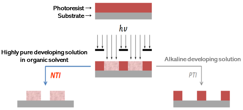
Fig. 3 Development process
Never-ending technological evolution
In the 2007 ITRS, functional diversification that appeared due to miniaturization limit theory was defined as More than Moore, in contrast to More Moore, which pursues Moore's law to the limit of miniaturization and high integration.
Different semiconductor manufacturers have different strategies, but currently, mass production of the latest 7-nm node generation has already begun applying an extreme ultraviolet (EUV) process, which enables continued miniaturization. The IRDS states that such size reduction trends will continue until 2028 and then proceed to three-dimensional very large scale integration (VLSI). Hence, further refinement of microstructures is being planned, and the chemicals applied to these processes are considered to require control at the ppq level, making it necessary to achieve further improvements in standard samples for determining the accuracy of measuring equipment and measurements.