Organic Electronics
Organic electronics is the collective term for technologies that utilize the electrons represented by electronic devices such as organic semiconductors. The electronic devices are prepared by printing or applying organic compounds on a plastic substrate, thereby they are light, soft and flexible. If there is advancement in these technologies, they are expected to be used in displays and wearable products.
FUJIFILM Wako deal with various functional materials that can be utilized for organic transistors, organic EL materials, and solar batteries.
Product Line-up
More Information
The history of fullerenes & carbon nanotubes (CNT)
-
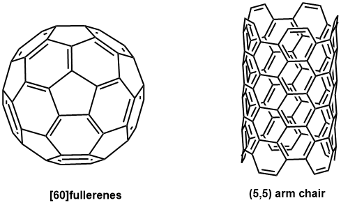
Fig. 1 The structures of fullerene & carbon nanotube -

Fig. 2 Graphite & diamond
Fullerenes and carbon nanotubes (Fig. 1) are called “carbon allotropes” like diamond and graphite. They are compounds made only of carbon element C. (Fig. 2)
Fullerenes have a spherical, hollow structure like soccer balls and rugby balls. Moreover, there are various types of fullerenes depending on the number of carbons. The most typical fullerene is C60, but there are also larger ones such as C70, C76, and C78, which are collectively called “fullerenes”. On the other hand, carbon nanotubes have a tubular structure in which graphene is rolled into a cylindrical shape, and they are also hollow. Besides, there are also various types depending on the diameter and the number of layers.
Fullerenes and carbon nanotubes have a short history. Of the two substances, fullerene was discovered first. In November 1985, fullerene made his name known to the scientists by the accidental discovery of H.W. Kroto at Rice University.
At first, they were researchers of the interstellar medium. In the experiment of the purpose for identifying the interstellar medium, they shined a high laser beam on the carbon plate, evaporated the carbon plate onto the cluster, and cooled it with helium gas. When they checked the TOF-MS of the product, they found a very large peak with a mass number of 720.1)
They sought a compound with a mass number of 720 and came to the conclusion that it was a soccer ball shaped spherical material consisting of a 5-membered ring and a 6-membered ring, which was published in Nature magazine that year. Besides, when this molecule was found, it named “ fullerene” after famous architect ‘ B. Fuller ‘ who construct dome shaped architecture.2)
While various chemists challenged the synthesis of fullerenes, in 1990 W. Kretschmer succeed in synthesizing fullerenes by the arc discharge method3) and the method was prevailed in the world. This was a major turning point in fullerene research because this method was able to produce stable fullerenes, which is known as the best method for producing C60 fullerenes to date.
Moreover, in 1991, the superconductivity of Tc = 18K was reported for K3C60, which was potassium-doped with C60, which triggered further fullerene research.4) This high-temperature superconducting property provoled increasing research on fullerene substances, and there were times when 2500 fullerene papers were published annually.5)
On the other hand, carbon nanotube was discovered by S. Iijima in 1991, which was six years after the research report of C60.6) At first, he tried to find out the structure of C60 fullerenes by applying arc discharge to carbon. He was conducting research to examine the soot there with an electron microscope. When he was observing fullerenes by the microscope, he found something like elongated crystals mixed with fullerenes, which were carbon nanotubes. (Fig. 3)
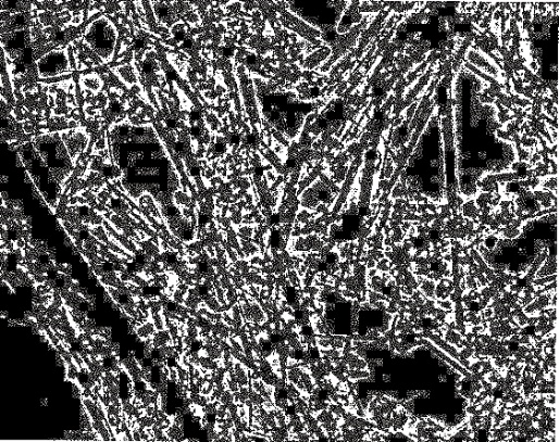
Fig. 3 The image of transmission electron microscope
Elongated crystals (carbon nanotube) can be seen mixed with black grains (fullerene).
(Source ; K. Tanaka, “carbon nanotube device heno tyosen”, Tokyo kagaku dojin, p4.)
Initially, this discovery received little attention. However, inspired by the discovery of C60 and the news of the superconducting effect of metal-encapsulated fullerene, research on carbon nanotubes has accelerated. Moreover, by the discovery of single nanotube in 1993,7) and the establishment of a mass synthesis method for carbon nanotube in 1996,8) it has attracted a great deal of attention, and research papers of carbon nanotube increased explosively, the number was about the same with fullerene’s paper.
The practical example and future prospects of fullerene and carbon nanotube
With the advent of fullerenes and carbon nanotube, the field of carbon functional materials has expanded. Fullerene and carbon nanotube have special structure and show strange physical prospects, so it has become clear that these are extremely useful as carbon functional materials.
Since fullerene can be doped with alkali metals to obtain superconductors, a great deal of research has been conducted on the development of superconductors with a high critical temperature. In addition, it has been proved to have photoconductivity 9), and it has also been found to have a photosensitizing function and a photo-induced rectification function. It is also applied to the field of optical functional materials such as photoelectric conversion devices. 10) In 2018, Y. Matsuo (the University of Tokyo) reported the life of the solar cells came to be improved by 10 times compared to the normal perovskite type solar cell by introducing Li-encapsulated fullerene in the perovskite type solar cells 11) (Fig. 4). It is also attracting attention in the medical field such as cancer treatment using cell-killing effect. 12)
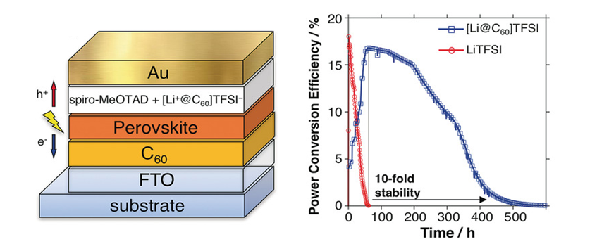
Fig. 4 Li+ @ C60 Doped perovskite solar cells
Jeon, I., Ueno, H., Seo, H., Aitola, K., Nishikubo, R., Saeki, A., Okada, H., Boschloo, G.,Maruyama, S., and Matsuo,Y. : Angew.Chem.Int.Ed., 57, 4607 (2018). (Figure citations)
Also, in the field of magnetism, ferromagnetism was confirmed in the charge transfer complex TDAE-C60 with tetrakis (dimethyl amino) ethylene 13). Taking advantage of this characteristic, it is expected to be applied to high-density recording materials for next-generation memory and pharmaceutical production utilizing magnetism. (Fig. 5)
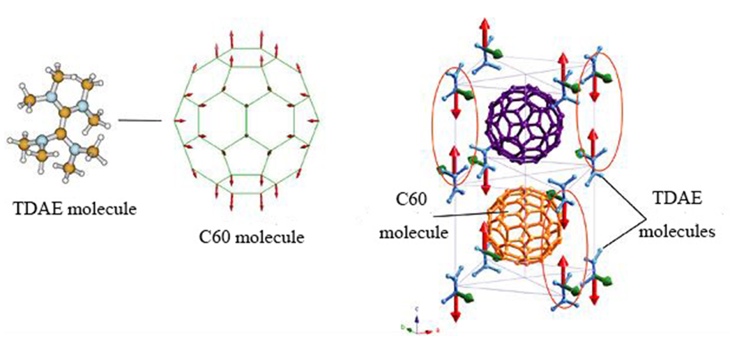
Fig. 5 The state of TDCA-C60 crystal in low temperature
(2011/10/25 : the Institute of Physical and Chemical Research; press release)
On the other hand, when considering the application of carbon nanotubes to materials, the most important one is their strength. Carbon nanotube have a highly complete structure in which a graphene sheet consisting of carbon covalent bonds is rolled into a cylindrical shape. They are excellent in thermal and chemical stability as well as strength. Furthermore, because it is a carbon material, it has excellent flexibility and maintains its original shape without breaking even when twisted. Taking advantage of these characteristics, it is expected to be applied to materials in the aerospace field that require high strength14) (Fig. 6), and flexible medical cameras15).
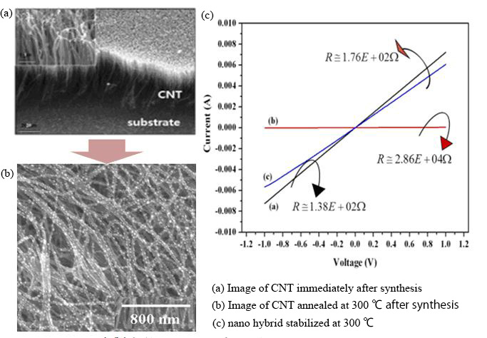
Fig. 6 CNT-metal nanoparticle complex for high sensitivity small sensors and their electrical propaties
(2021/4/1: JAXA Aeronautical Technology Directorate web site 14))
Carbon nanotube is also conductive substances like fullerene, so they can be used as transistors by attaching electrodes16), to make solar cells in combination with fullerene17)18)19), and as electronic devices in electronics, research is also underway from the perspective.
In this way, fullerenes and carbon nanotubes are not only “ interesting to be made of carbon and have an unusual shape”, but also have various practicalities. It may not be long before fullerenes and carbon nanotubes appear in your life.
References
- Kroto, H.W., Heath, J.R., O’Brien, S.C., Curl, R.F., and Smalley R.E.: Nature, 318, 162 (1985).
- Araki, K., Akashi, M., Takahara, J., Kudo, K.:”Yuki kinouzairyo”,Tokyokagakudojin, p.146 (2006).
- Kratchmer, W., Lamb, L.D., Fostiropoulos, K., and Huffman, D.R.: Nature, 347, 354 (1990).
- a) Haddon, R.C. et al.:Nature, 350, 320 (1991). b) Hebard, A.F., et al.:Nature, 350, 600 (1991).
- The Chemical Society of Japan, “Tanso daisan no dousotai fullerene no kagaku”, p.8 (1999).
- Iijima, S.: Nature, 352, 56 (1991).
- Ajayan, P.M., and Iijima, S.: Nature, 361, 333 (1993).
- Yakobson, B., Smalley, R.E.: Am. Sci., 85, 324 (1997).
- Minami, N.: Chem. Lett., 20, 1791 (1991).
- Kanefuji, K.: “kagaku to kogyo”, 45, 902 (1995).
- Jeon, I., Ueno, H., Seo, S., Aitola, K., Nishikubo, R., Saeki, A. Okada, H., Boschloo, G., Maruyama, S., and Matsuo, Y.: Angew. Chem. Int. Ed., 57, 4607 (2018).
- Tabata,Y., Ikada,Y.: Pure Appl. Chem., 71, 2047 (1999).
- Yamaoka, H., Kambe, T., Sato, T., Ishida, Y., Matsunami, M., Eguchi, R., Senba, Y., and Ohashi, H.: Physical Review B(Rapid Communication),84, 161404(R) (2111).
- JAXA Aeronautical Technology Directorate web site
- Suzuki, D., Oda, S., and Kawano,Y. : Nat. Photonics., 10, 809 (2016).
- Yao, Z., Postma, H.W.Ch., Balents,L., andDekker,C., Nature, 402, 273 (1999)..
- Ago, H., Komatsu,T., Ohshima,S., Kuriki,Y., Yumura, M.: Appl. Phys. Lett., 77, 79 (2000).
- Jeon, I., Cui, K., Chiba, T., Anisimov, A., Nasibulin,A.G., Kauppinen, E.I., Maruyama, S., Matsuo, Y.: J. Am. Chem. Soc.,137, 7982 (2015).
- Jeon, I., Seo, S., Sato, Y., Delacou, C., Anisimov, A., Suenaga, K., Kauppinen, E.I., Maruyama, S., Matsuo, Y., J. Phys. Chem. C., 121, 25743 (2017).
Product Line-up
For research use or further manufacturing use only. Not for use in diagnostic procedures.
Product content may differ from the actual image due to minor specification changes etc.
If the revision of product standards and packaging standards has been made, there is a case where the actual product specifications and images are different.
The prices are list prices in Japan.Please contact your local distributor for your retail price in your region.