p-Type Organic Semiconductors
Organic field-effect transistors (OFETs) have been good attentions as mechanically flexible and lightweight materials. Printed flexible devices for active layer made from organic semiconductor materials can be manufactured by means of low-cost and environment-friendly coating processes, and are particularly expected as next-generation electronics.
A newly line-up of highly soluble p-type semiconductor materials with high hole mobility is available from FUJIFILM Wako. These products are new materials developed by the joint research with Prof. Dr. Takeya and Assoc. Prof. Dr. Okamoto of The University of Tokyo and FUJIFILM Corporation.
Features
- High hole mobility
The hall mobility is over 5 cm2/Vs. - High heat resistance
The products do not deteriorate even when used at the temperature required for OSC patterning. - High solubility
Solubility in toluene : 0.5 wt% - High repeatability
Good repeatability was confirmed in the characterization of the transistor by Pi-Crystal, Inc. - Sublimated products
The purity of over 99% is guaranteed
Summary of various transistor element characteristics
-
Film production method Substrate temperature(℃) µmax
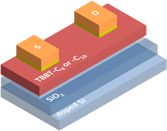
(cm2/Vs)aVth (V)b Ion/ Ioff Drop-casting 40 4.0 -21 - -37 106 Edge-casting 40 6.2 -15 - -20 106 Vacuum deposition 60 1.8 -15 - -20 106 100 1.0 -15 - -20 106 a)Evaluated in the saturation region. b) The gate insulator is SiO2 with a thickness of 200 nm.
-
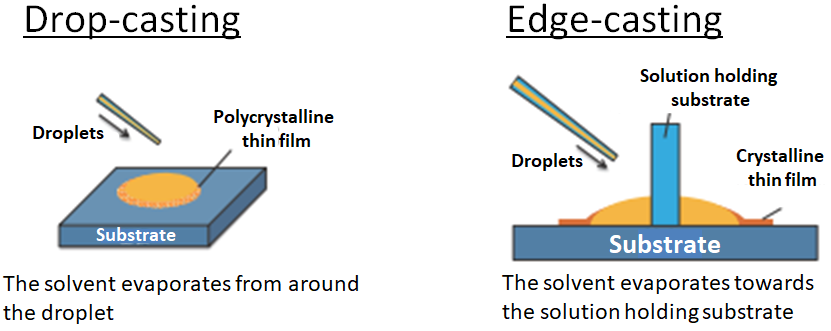
Crystal film fabrication by edge casting method and transistor characterization evaluation
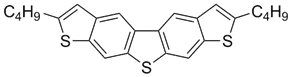
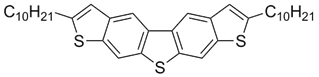
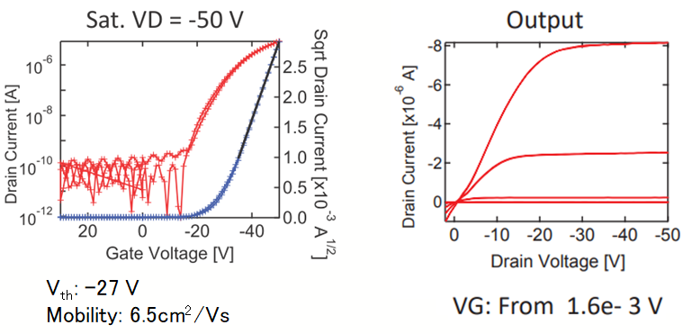
TBBT-C4
-
-
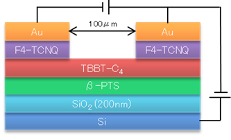
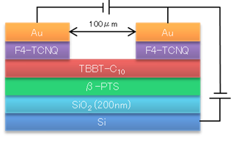
Coating film formation conditions Solvent Toluene Concentration 0.05 wt% Melted temperature 60 ℃ Hot plate temperature 50 ℃ Substrate SiO2 200 nm SAM β-PTS Drop amount 1 drop Drying Under pressure, 50℃, 8h
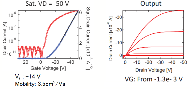
TBBT-C10
-
-
Coating film formation conditions Solvent Anisole Concentration 0.05 wt% Melted temperature 70 ℃ Hot plate temperature 40 ℃ Substrate SiO2 200 nm SAM β-PTS Drop amount 1 drop Drying Under pressure, 70℃, 24h
References
- Okamoto, T. and Takeya, J. et al.: Adv. Mater., 25, 6392 (2013).
- Okamoto, T. et al.: J. Mater. Chem. C, 5, 1903 (2017).
Product List
- Open All
- Close All
p-Type Organic Semiconductors
n-Type Organic Semiconductors
Organic Semiconductor Building Block
For research use or further manufacturing use only. Not for use in diagnostic procedures.
Product content may differ from the actual image due to minor specification changes etc.
If the revision of product standards and packaging standards has been made, there is a case where the actual product specifications and images are different.
The prices are list prices in Japan.Please contact your local distributor for your retail price in your region.